NT5CB256M16DP-EK Datasheet: Complete 4Gb DDR3 Specs & Pinout Guide
Struggling to integrate the NT5CB256M16DP-EK into your automotive or industrial design? This 4Gb DDR3 SDRAM offers robust performance, but mastering its DDR3 Specs and complex pin mapping is critical for signal integrity. This guide cuts through the datasheet noise, providing a streamlined solution for engineers needing accurate configuration data and a clear Pinout Guide to accelerate development cycles.
Core Technical Specifications Overview

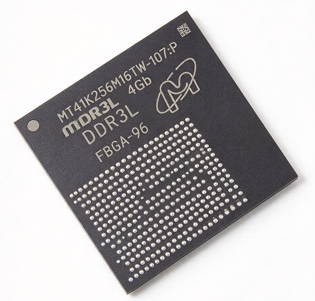
You need to grasp the fundamental architecture of this memory component before diving into layout details. The NT5CB256M16DP-EK represents a significant density jump in the DDR3 landscape, offering 4 gigabits of storage capacity organized in a x16 bit width configuration. Understanding these core parameters ensures that you select the right operating conditions for your specific application environment.
Memory Architecture and Density Details
The device utilizes a 256 Megabit by 16-bit organization, effectively storing 4Gb of data. You will find that this high-density structure requires precise address mapping. Unlike lower-density parts, the internal bank structure consists of eight banks, which allows for parallel access patterns. This architecture supports burst lengths of 8, ensuring efficient data transfer rates when interfacing with modern controllers.
Operating Voltage and Speed Grades
Power consumption and speed are tightly coupled in this component. The part operates at a nominal voltage of 1.5V, adhering to standard DDR3 specifications. However, it also supports low-voltage variants depending on the specific suffix code interpretation. You must verify the speed grade, typically ranging from 1066 Mbps to 1600 Mbps. Selecting the correct speed bin is vital for meeting system timing requirements without inducing excessive heat.
Comprehensive Pinout and Signal Mapping
Correct pin assignment is non-negotiable for successful integration. A miswired control line can lead to catastrophic initialization failures. The following sections break down the critical groups within the Pinout Guide, helping you map each physical pin to its logical function within the controller interface.
Power, Ground, and Control Pin Assignments
Stable power delivery is the foundation of reliable operation. The VDD and VDDQ pins supply the core and I/O circuits, respectively. You must ensure proper decoupling capacitor placement near these pins to filter out high-frequency noise. The ground network (VSS) provides the reference potential. Control pins such as CS# (Chip Select), RAS#, CAS#, and WE# dictate the command sequence. Incorrect logic levels on these lines during initialization will prevent the memory from entering ready mode.
Data Bus and Address Line Configuration
The data bus consists of sixteen bidirectional pins (DQ0-DQ15). You should treat these lines as high-speed differential pairs where possible, though they operate single-endedly in standard DDR3. Address lines (A0-A15) determine the location of the data within the memory array. Note that higher-order address bits may be shared with other functions depending on the specific row/column multiplexing scheme defined in the datasheet. Always double-check the address latch enable (ALE) functionality if your controller supports it.
| Pin Group | Function | Critical Consideration |
|---|---|---|
| DQ[15:0] | Data Input/Output | Match trace lengths for skew minimization. |
| A[15:0] | Address Inputs | Verify multiplexed Row/Column addressing. |
| VDD/VDDQ | Power Supply | Requires local bypass capacitors (<10nF). |
| CK/CK# | Clock Inputs | Differential pair; strict impedance control needed. |
Timing Parameters and Performance Metrics
Performance hinges on respecting strict timing windows. You cannot simply connect the chip and expect it to work; the controller must issue commands within specific timeframes relative to the clock edge. These parameters define the latency and throughput characteristics of the subsystem.
Critical Latency Timings (CL, tRCD, tRP)
Three key timings dominate performance calculations. CAS Latency (CL) defines the delay between the read command and the first data output. Typically, this ranges from 7 to 11 cycles depending on the speed grade. tRCD (RAS to CAS Delay) measures the time required to activate a row before reading or writing. tRP (Row Precharge Time) dictates how long it takes to close a row before opening another. You must configure your memory controller’s timing registers to match these values exactly, or data corruption will occur.
Refresh Rates and Power-Down Modes
DDR3 SDRAM requires periodic refresh cycles to maintain data integrity. The standard refresh interval is every 7.8 microseconds for normal temperature operation. Failure to issue REFRESH commands results in data loss. Additionally, the device supports various power-down modes. In deep power-down mode, the DLL is disabled, and current consumption drops significantly. You should leverage these modes during idle periods to optimize overall system power efficiency, especially in battery-operated devices.
Design Implementation Best Practices
Translating datasheet specs into a working PCB requires careful attention to signal integrity. High-speed memory interfaces are sensitive to impedance mismatches and crosstalk. Following established guidelines ensures stable operation across all process corners and temperatures.
PCB Layout Guidelines for High-Speed Signals
Keep traces short and direct. You should minimize stubs on the address and control buses. Use a solid ground plane beneath the memory layer to provide a consistent return path. For the clock signals (CK and CK#), maintain tight coupling and equal length. Avoid routing these critical signals over split planes or vias that disrupt the return current flow. Layer stack-up planning is essential; aim for controlled impedance of 50 ohms for single-ended lines and 100 ohms for differential pairs.
Termination Strategies and Impedance Matching
Proper termination prevents reflections that degrade signal quality. DDR3 uses ODT (On-Die Termination) internally, but external termination resistors are still often required on the controller side or for fly-by topologies. You must calculate the appropriate resistor values based on the trace impedance and driver strength. Typically, parallel termination is used for point-to-point connections, while series termination might be employed for longer runs. Verify that the termination scheme matches your specific topology to maximize signal margins.
Environmental Compliance and Reliability
Long-term reliability depends on operating within specified environmental limits. Industrial and automotive applications demand rigorous adherence to temperature and longevity standards. Ignoring these factors can lead to premature field failures.
Temperature Range and Automotive Grade Standards
The commercial grade typically operates from 0°C to +85°C. However, extended temperature ranges are available for harsher environments. If you are designing for automotive use, look for AEC-Q100 qualified variants. These parts undergo rigorous testing for thermal cycling and humidity resistance. Ensure your thermal management strategy keeps the junction temperature within the absolute maximum ratings, even under heavy load conditions.
Longevity and Obsolescence Management
Memory components have finite lifecycle support. You should monitor product change notices (PCNs) regularly. Nanya Technology provides long-term availability guarantees for certain industrial parts, but you must verify the status of the specific SKU. Plan for alternative sources or redesign contingencies if the part approaches end-of-life. Maintaining a buffer stock for critical production runs can mitigate supply chain disruptions associated with obsolete components.
Key Takeaways
- Master the NT5CB256M16DP-EK Datasheet by focusing on its 4Gb density and x16 architecture for optimal controller configuration.
- Adhere strictly to the Pinout Guide for power and control lines to prevent initialization failures and ensure signal integrity.
- Configure timing parameters like CL, tRCD, and tRP accurately to meet performance targets and avoid data corruption.
- Implement robust PCB layout practices with controlled impedance and proper termination to handle high-speed DDR3 signals.
- Consider environmental grades and obsolescence management for long-term reliability in industrial and automotive applications.
Frequently Asked Questions
What is the primary advantage of the NT5CB256M16DP-EK?
The main advantage is its 4Gb density in a x16 configuration, allowing for high-capacity memory solutions without requiring multiple chips. This simplifies board layout and reduces the total number of components needed for large memory arrays, making it ideal for space-constrained designs.
How do I interpret the speed grade in the datasheet?
The speed grade indicates the maximum data rate supported, such as DDR3-1600. You must check the timing table for specific CL values at that frequency. Higher speed grades require stricter signal integrity controls and potentially more aggressive termination strategies to maintain stability.
Can this part operate in low-power modes?
Yes, the device supports self-refresh and power-down modes. In self-refresh, the memory maintains data with minimal power consumption, which is crucial for battery-backed systems. Properly configuring the CKE pin allows you to enter these states seamlessly during idle periods.
What are the critical PCB layout guidelines for this component?
Keep traces short and direct, minimize stubs on address/control buses, and use a solid ground plane. Maintain tight coupling and equal length for clock signals (CK/CK#). Aim for controlled impedance of 50 ohms for single-ended lines and 100 ohms for differential pairs to prevent reflections and crosstalk.