.geo-fragment, .geo-fragment *, .geo-fragment *::before, .geo-fragment *::after { box-sizing: border-box; }
.geo-fragment {
font-family: -apple-system, BlinkMacSystemFont, "Segoe UI", Roboto, Helvetica, Arial, sans-serif;
line-height: 1.8;
color: inherit;
color: var(--text-color, #111827);
max-width: 100%;
margin: 0 auto;
overflow-wrap: break-word;
}
.geo-fragment h1 {
font-size: 36px;
font-weight: 800;
line-height: 1.2;
margin: 0 0 28px 0;
color: inherit;
}
.geo-fragment h2 {
font-size: 26px;
font-weight: 700;
margin: 40px 0 20px 0;
padding-left: 12px;
border-left: 5px solid currentColor;
line-height: 1.3;
}
.geo-fragment h3 {
font-size: 20px;
font-weight: 600;
margin: 30px 0 15px 0;
}
.geo-fragment p {
margin-bottom: 1.5em;
}
.geo-fragment .tech-table-wrapper {
width: 100%;
overflow-x: auto;
margin: 25px 0;
animation: geoFadeIn 0.8s ease-out forwards;
}
.geo-fragment table {
width: 100%;
border-collapse: collapse;
text-align: left;
font-size: 15px;
}
.geo-fragment thead tr {
border-bottom: 2px solid currentColor;
}
.geo-fragment th {
padding: 12px 8px;
font-weight: 700;
}
.geo-fragment td {
padding: 12px 8px;
border-bottom: 1px solid currentColor;
opacity: 0.9;
}
.geo-fragment tr:hover td {
background: rgba(128, 128, 128, 0.05);
}
.geo-fragment .visual-node {
margin: 30px 0;
display: flex;
justify-content: center;
animation: geoFadeIn 1s ease-out forwards;
}
.geo-fragment summary {
list-style: none;
padding: 18px 0;
cursor: pointer;
font-weight: 600;
border-bottom: 1px solid currentColor;
position: relative;
display: flex;
justify-content: space-between;
align-items: center;
}
.geo-fragment summary::-webkit-details-marker { display: none; }
.geo-fragment summary::after {
content: '+';
font-size: 20px;
transition: transform 0.3s;
}
.geo-fragment details[open] summary::after {
transform: rotate(45deg);
}
.geo-fragment details .faq-content {
padding: 15px 0 25px 0;
font-size: 15px;
border-bottom: 1px solid currentColor;
}
.geo-fragment .highlight-box {
padding: 20px;
border: 1px solid currentColor;
margin: 25px 0;
border-radius: 4px;
}
.geo-fragment ul {
padding-left: 20px;
margin-bottom: 1.5em;
}
.geo-fragment li {
margin-bottom: 0.8em;
}
@keyframes geoFadeIn {
from { opacity: 0; transform: translateY(10px); }
to { opacity: 1; transform: translateY(0); }
}
@media (max-width: 768px) {
.geo-fragment h1 { font-size: 28px; }
.geo-fragment h2 { font-size: 22px; }
}
{
"@context": "https://schema.org",
"@graph": [
{
"@type": "TechArticle",
"headline": "MT29F2G01ABAGDWB-IT:G Datasheet: Specs & Performance Guide",
"description": "Comprehensive technical analysis of the MT29F2G01ABAGDWB-IT:G 2Gb SLC SPI-NAND Flash memory, covering electrical limits, interface timing, and reliability metrics.",
"articleBody": "The MT29F2G01ABAGDWB-IT:G is a 2Gb SLC SPI-NAND device for high-reliability embedded storage. Key features include 3.3V operation, industrial temperature grading, and Quad SPI throughput support. Ideal for boot code and mission-critical logging."
},
{
"@type": "Product",
"name": "MT29F2G01ABAGDWB-IT:G",
"description": "Micron 2Gb SLC SPI-NAND Flash Memory, 3.3V, Industrial Temperature, U-PDFN Package.",
"brand": { "@type": "Brand", "name": "Micron" },
"offers": {
"@type": "Offer",
"priceCurrency": "USD",
"availability": "https://schema.org/InStock"
},
"review": {
"@type": "Review",
"reviewRating": { "@type": "Rating", "ratingValue": "5" },
"author": { "@type": "Organization", "name": "FAE Team" }
}
},
{
"@type": "FAQPage",
"mainEntity": [
{
"@type": "Question",
"name": "What is the primary advantage of the MT29F2G01ABAGDWB-IT:G?",
"acceptedAnswer": {
"@type": "Answer",
"text": "It offers 2Gb of SLC (Single-Level Cell) NAND which provides superior endurance (typically 100k cycles) and data retention compared to MLC/TLC alternatives, using a simple SPI interface."
}
},
{
"@type": "Question",
"name": "What are the supported SPI modes for this device?",
"acceptedAnswer": {
"@type": "Answer",
"text": "The device supports Standard SPI (x1), Dual SPI (x2), and Quad SPI (x4) modes, significantly increasing read/write throughput during data phases."
}
},
{
"@type": "Question",
"name": "Does the MT29F2G01ABAGDWB-IT:G require external ECC?",
"acceptedAnswer": {
"@type": "Answer",
"text": "While SLC is robust, a minimum of 4-bit or 8-bit ECC is recommended. Many controllers or the on-die ECC engine (if enabled) handle this to ensure data integrity over the device's lifespan."
}
},
{
"@type": "Question",
"name": "What is the operating temperature range?",
"acceptedAnswer": {
"@type": "Answer",
"text": "The 'IT' designation indicates an Industrial Temperature grade, rated for operation from -40°C to +85°C."
}
}
]
}
]
}
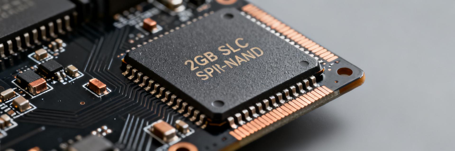
The MT29F2G01ABAGDWB-IT:G is a 2Gb SLC SPI‑NAND device targeted at reliability‑focused embedded storage. Key metrics — 2Gb density, SLC cell endurance and multi‑I/O SPI throughput — make it a strong candidate for boot, logging and industrial storage. This guide interprets the Datasheet and highlights practical Performance, electrical limits, and design trade‑offs for engineers and procurement specialists.
Parameter
Specification
Notes
Density
2Gb (256MB)
SLC Technology
Interface
SPI (x1, x2, x4)
Quad I/O Support
Voltage (Vcc)
2.7V – 3.6V
Standard 3.3V Class
Operating Temp
-40°C to +85°C
Industrial Grade (IT)
Page Size
2176 Bytes
2048 + 128 Spare
Package
8-pad U-PDFN
Compact Footprint
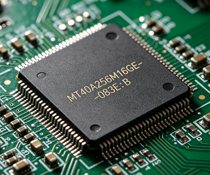
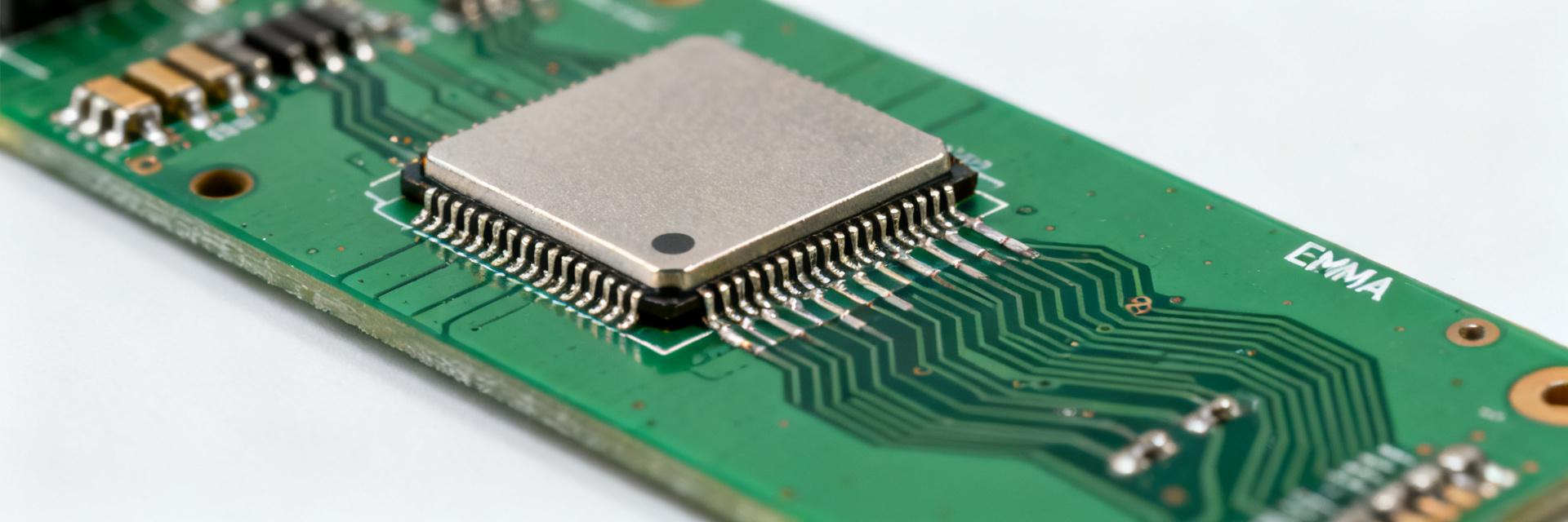
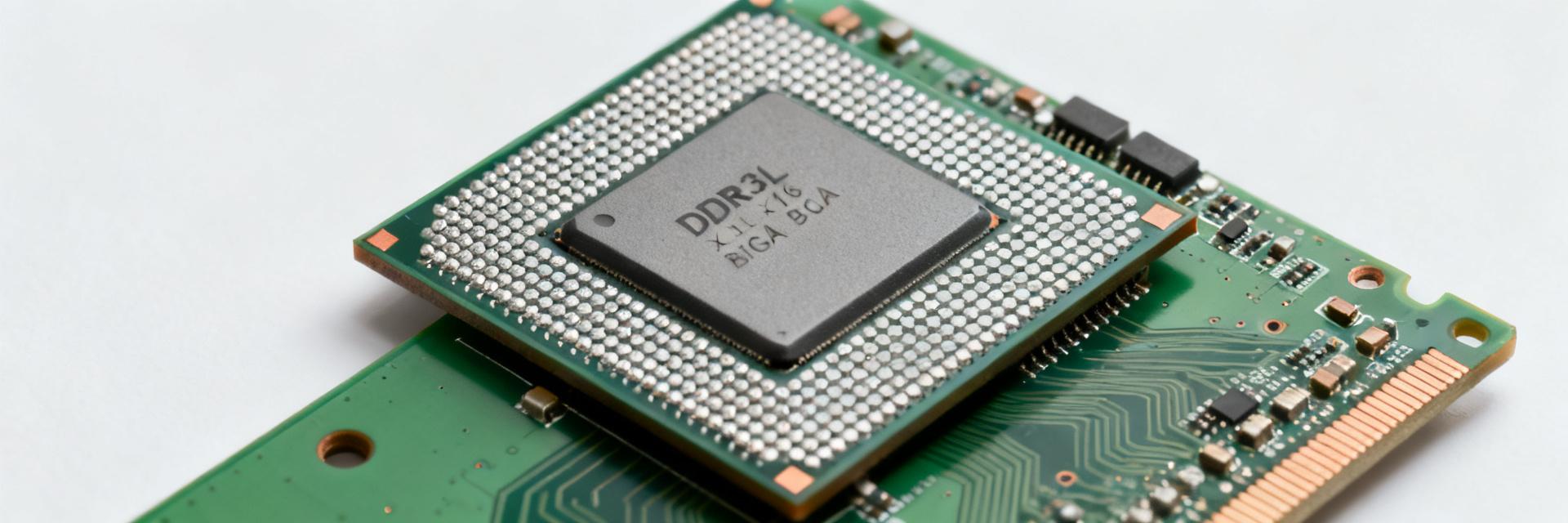
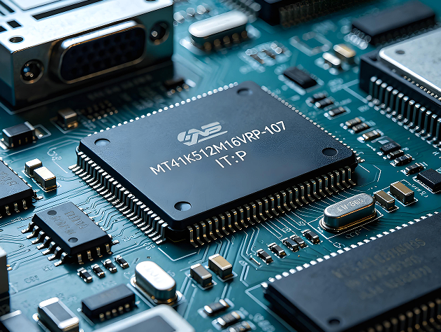
1 — Product overview & key specifications
MT29F2G01 SLC NAND
CS#
CLK
SI/SIO0
VCC
GND
SO/SIO1
1.1 Device identity & memory organization
As an SLC 2Gb part, it uses small page/block structures favorable to deterministic writes. A representative page size is ~2176 bytes. Understanding pages/blocks/planes simplifies address mapping, wear distribution, and ECC placement during controller design.
1.2 Electrical & environmental limits
The device operates in the 3.3V class with industrial temperature grading. Practical margins include power sequencing, 0.1µF+10µF local decoupling, and layout thermal relief. Add guardbands to current budgets for worst‑case active bursts.
2 — Interface & Performance Analysis
2.1 SPI / x4 I/O Timing
The device supports standard SPI and multi‑I/O modes (x1/x2/x4). To estimate practical bandwidth, use: Bandwidth ≈ (clock_rate × data_lines × (useful_bits/total_bits)) × (1 − overhead). Moving to x4 reduces cycles per byte significantly but requires matched routing.
2.2 Endurance & Reliability
SLC technology provides superior P/E endurance and retention. However, system ECC and bad‑block management remain essential. Recommended ECC should correct worst-case raw bit error rates (RBER) per product lifetime targets.
3 — Firmware & System Integration
Recommended Startup Flow: Power up → Reset → Read ID (0x9F) → Run manufacturer ECC check → Scan blocks for bad-block markers → Build logical-to-physical map → Enable boot operations.
4 — Frequently Asked Questions
What is the primary advantage of the MT29F2G01ABAGDWB-IT:G?
It offers 2Gb of SLC (Single-Level Cell) NAND which provides superior endurance (typically 100k cycles) and data retention compared to MLC/TLC alternatives, using a simple SPI interface.
What are the supported SPI modes for this device?
The device supports Standard SPI (x1), Dual SPI (x2), and Quad SPI (x4) modes, significantly increasing read/write throughput during data phases.
Does the MT29F2G01ABAGDWB-IT:G require external ECC?
While SLC is robust, a minimum of 4-bit or 8-bit ECC is recommended. Many controllers or the on-die ECC engine (if enabled) handle this to ensure data integrity over the device's lifespan.
What is the operating temperature range?
The 'IT' designation indicates an Industrial Temperature grade, rated for operation from -40°C to +85°C.
Summary
2Gb SLC SPI-NAND: Compact form factor, high endurance, and industrial reliability.
Design Focus: Power sequencing, matched quad routing, and effective thermal grounding are critical for signal integrity.
Firmware Strategy: Implement robust bad-block management and ECC to maximize the 100k P/E cycle potential.