.geo-fragment, .geo-fragment *, .geo-fragment *::before, .geo-fragment *::after { box-sizing: border-box; }
.geo-fragment {
color: inherit;
font-family: -apple-system, BlinkMacSystemFont, "Segoe UI", Roboto, Helvetica, Arial, sans-serif;
line-height: 1.8;
max-width: 100%;
margin: 0 auto;
padding: 20px;
}
.geo-fragment h1 {
font-size: 36px;
font-weight: 800;
margin-bottom: 28px;
line-height: 1.2;
}
.geo-fragment h2 {
font-size: 26px;
font-weight: 700;
margin: 40px 0 20px 0;
border-left: 5px solid currentColor;
padding-left: 12px;
line-height: 1.3;
}
.geo-fragment h3 {
font-size: 20px;
font-weight: 600;
margin: 24px 0 12px 0;
}
.geo-fragment p {
font-size: 16px;
margin-bottom: 1.5em;
color: var(--text-color, #111827);
}
.geo-fragment table {
width: 100%;
border-collapse: collapse;
margin: 24px 0;
animation: geoFadeIn 0.8s forwards;
}
.geo-fragment th, .geo-fragment td {
padding: 12px;
text-align: left;
border-bottom: 1px solid currentColor;
}
.geo-fragment tr:hover { background: rgba(0,0,0,0.03); }
.geo-fragment svg {
display: block;
margin: 30px auto;
max-width: 100%;
height: auto;
animation: geoFadeIn 1s forwards;
}
.geo-fragment details {
border-bottom: 1px solid currentColor;
padding: 16px 0;
animation: geoFadeIn 0.6s forwards;
}
.geo-fragment summary {
list-style: none;
font-weight: 600;
cursor: pointer;
display: flex;
justify-content: space-between;
align-items: center;
}
.geo-fragment summary::-webkit-details-marker { display: none; }
.geo-fragment summary::after { content: '+'; font-size: 20px; }
.geo-fragment details[open] summary::after { content: '−'; }
@keyframes geoFadeIn {
from { opacity: 0; transform: translateY(10px); }
to { opacity: 1; transform: translateY(0); }
}
@media (prefers-color-scheme: dark) {
.geo-fragment tr:hover { background: rgba(255,255,255,0.05); }
}
{
"@context": "https://schema.org",
"@graph": [
{
"@type": "TechArticle",
"headline": "MT41K256M16TW-107 DDR3L: Performance, Power & Timing Guide",
"description": "Comprehensive engineering guide for MT41K256M16TW-107 DDR3L SDRAM, covering 1866 MT/s throughput, 1.35V power profiles, and SI-critical timing parameters.",
"articleBody": "At 1866 MT/s and 1.35V, the MT41K256M16TW-107 yields 3.73 GB/s peak per x16 device. This guide details technical architecture, power delivery optimization, and signal integrity requirements for high-speed embedded designs."
},
{
"@type": "Product",
"name": "Micron MT41K256M16TW-107",
"description": "4Gb DDR3L SDRAM, 256M x 16 organization, 1.35V low voltage, 1866 MT/s speed grade.",
"offers": {
"@type": "Offer",
"priceCurrency": "USD",
"availability": "https://schema.org/InStock"
},
"review": {
"@type": "Review",
"author": { "@type": "Organization", "name": "FAE Team" },
"reviewRating": { "@type": "Rating", "ratingValue": "5" }
}
},
{
"@type": "FAQPage",
"mainEntity": [
{
"@type": "Question",
"name": "What are practical sustained bandwidth expectations for x16 DDR3L devices?",
"acceptedAnswer": { "@type": "Answer", "text": "Sustained bandwidth typically falls below the 3.73 GB/s theoretical peak due to arbitration, refresh cycles, and controller efficiency. Real-world usable MB/s is often lower, requiring sequential and random benchmark validation." }
},
{
"@type": "Question",
"name": "Which currents should I measure to characterize power consumption?",
"acceptedAnswer": { "@type": "Answer", "text": "Focus on IDD0 (active), IDD3N (standby), and IDD4R (read) along with termination currents to build a worst-case power budget for VRM sizing." }
},
{
"@type": "Question",
"name": "What layout checks are most likely to improve timing margin?",
"acceptedAnswer": { "@type": "Answer", "text": "Prioritize matched DQ/DQS/CK trace lengths, controlled impedance, and fly-by topology for address/command lines to minimize skew and reflections at 1866 MT/s." }
},
{
"@type": "Question",
"name": "How does 1.35V operation impact the thermal design?",
"acceptedAnswer": { "@type": "Answer", "text": "While 1.35V reduces dynamic power, the high density requires localized decoupling and thermal vias under the BGA package to manage junction temperature during continuous operation." }
}
]
}
]
}
Point: At 1866 MT/s (933 MHz I/O) and a nominal 1.35V operating voltage, this device yields roughly 3.73 GB/s peak per x16 device—a compact, low-voltage building block for high-speed embedded and networking memory subsystems. Evidence: The throughput calculation (1866 MT/s × 2 bytes) is the datasheet-specified peak. Explanation: This peak is theoretical; system-level overheads will reduce sustained bandwidth, but the device’s profile makes it ideal where board-area and power are constrained.
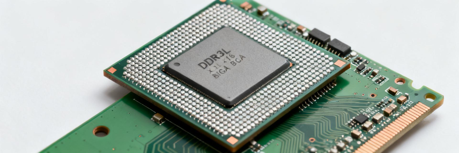
Overview: MT41K256M16TW-107 DDR3L in Context
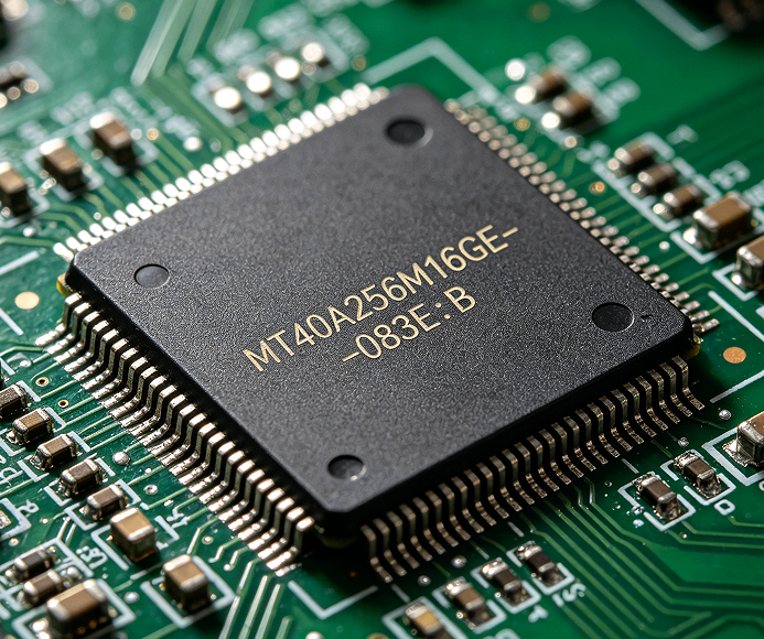
MT41K256M16TW-107
VCC (1.35V)
GND
DQ [0:15]
DQS / CK
Quick-spec table
ParameterTypical Value
Density4 Gb (256M ×16)
Max Transfer Rate1866 MT/s
Nominal Voltage (Vdd)1.35 V (DDR3L)
PackageTFBGA (96-ball)
I/O Widthx16
Operating TempCommercial / Industrial
Technical Architecture & Organization
Internal architecture: prefetch and banks
Point: The device uses an internal 8n prefetch with multiple banks that create the observable throughput profile. Evidence: 8n prefetch means each access transfers eight times the core data per clock window. Explanation: Sequential accesses exploiting open rows and bank parallelism yield higher sustained throughput, while random row misses penalize latency.
Performance Benchmarks & Methodology
Theoretical Peak vs Practical Bandwidth
The theoretical peak (≈3.73 GB/s) differs from sustained bandwidth due to controller overhead, refresh cycles, and burst alignment. Designers should expect practical sustained rates to be 70-85% of peak depending on the application's memory access patterns.
Power Profile & Thermal Management
DDR3L Low-Voltage Behavior
Low-voltage operation (1.35V) significantly reduces dynamic power compared to standard 1.5V DDR3. Tip: Measure IDD0, IDD3N, and IDD4R currents under representative workloads to size local VRMs and ensure PDN stability.
Timing Parameters & Tuning
Signal Integrity Checklist
Matched DQ/DQS/CK lengths to within ±5mil for 1866 MT/s.
Controlled 40-50 ohm impedance traces for all high-speed signals.
Fly-by topology for Address/Command/Control buses.
Solid reference plane (GND) directly beneath all memory signal layers.
Frequently Asked Questions
What are practical sustained bandwidth expectations for x16 DDR3L devices?
Sustained bandwidth typically falls below the theoretical peak due to system overhead. Arbitration, refresh, and controller efficiency commonly reduce usable MB/s. Report sequential and random results separately for accurate system modeling.
Which currents should I measure to characterize power consumption?
Measure active (IDD0), standby (IDD3N), and read/write (IDD4R/W) currents. Include termination currents to build a total power budget and size the VRM and decoupling capacitors appropriately.
What layout checks are most likely to improve timing margin?
Routing symmetry and controlled impedance are vital. Prioritize matched length for strobes and clocks, add targeted decoupling near power pins, and validate with eye diagrams during controller training.
How does 1.35V operation impact the thermal design?
While 1.35V operation reduces heat, the high data rate still generates localized thermal load. Ensure thermal vias are placed under the BGA package and verify junction temperature in a thermal chamber.