MT40A512M16LY-075:E DDR4 Specs Deep Dive: Key Metrics
Introduction: Point — DDR4 performance continues to cluster in the 2400–2666 MT/s tiers with 1.2V nominal operation; evidence from supplier datasheets and system deployments shows these speeds dominate typical server and embedded platforms. Explanation — this article delivers an engineer-focused, metric-first breakdown of the MT40A512M16LY-075:E to support system selection and integration decisions for DDR4 SDRAM integration.
Point — scope and audience: evidence-driven engineers needing throughput, timing, power and validation guidance. Explanation — the following sections decode part nomenclature, walk through bandwidth and latency calculations, specify power/thermal limits, cover PCB/layout checklists, and give test pass/fail criteria for practical integration and risk trade-offs.
1 Part overview & nomenclature (Background introduction)
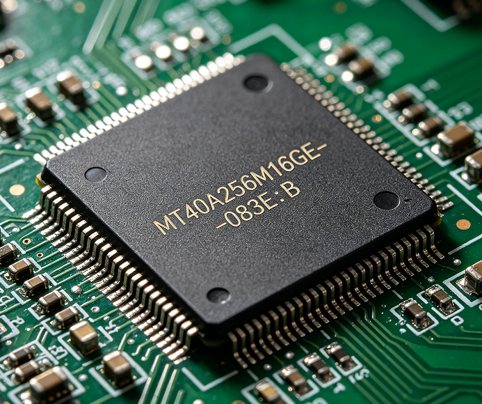
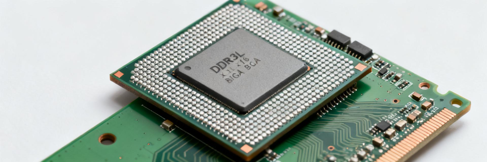
Part-number decoding and package details
Point — decode the identifier to reveal organization and capabilities. Evidence — MT40A512M16LY-075:E maps to an 8 Gbit density organized as 512M x 16 with a speed grade indicated by the suffix; Explanation — package metrics to call out include BGA ball count and pitch, FBGA package type, thermal pad presence, and pinout for VDD/VSS and command/address lanes; the MT40A512M16LY-075:E designation should be checked against the vendor datasheet when confirming package and speed.
Quick specs snapshot (at-a-glance table guidance)
Point — present essential numbers in a spec-summary box for rapid review. Evidence — the table below lists the core fields engineers should assemble from the datasheet. Explanation — triple-check timing, max data rate, and thermal limits on the official datasheet before final BOM sign-off.
| Field | Typical Value / Note |
|---|---|
| Density | 8 Gbit (512M x 16) |
| Data width | x16 per device |
| Nominal voltage | 1.2 V (DDR4 nominal) |
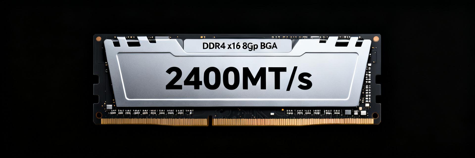
| Max data rate | Commonly 2400–2666 MT/s class (verify part marking) |
| Clock (fCK) | MT/s ÷ 2 (report in MHz) |
| Operating temp | 0°C to 95°C (check industrial vs. commercial grade) |
| Form factor | FBGA—note thermal pad and ballmap |
2 Performance metrics & timing parameters (Data analysis)
Data rate, bandwidth and throughput calculations
Point — convert MT/s and data width into effective bandwidth for design budgeting. Evidence — for a x16 device, bandwidth (GB/s) = (MT/s × 2 bytes) / 1000; Explanation — example: at 2400 MT/s a single x16 device yields ~4.8 GB/s (2400 × 2 = 4800 MB/s). For a 64-bit channel (four x16 devices) multiply by four to estimate peak channel throughput (~19.2 GB/s at 2400 MT/s). Annotate sustained vs. peak: sustained will be lower due to refresh, command overhead and open-page efficiency.
Latency and timing values to prioritize (CAS, tRCD, tRP, tRAS, tRFC)
Point — cycle counts must be translated to nanoseconds to assess real latency. Evidence — tCK = 1000 / (MT/s ÷ 2) in MHz units; Explanation — example: at 2400 MT/s, fCK ≈ 1200 MHz and tCK ≈ 0.833 ns, so CL15 ≈ 12.5 ns. Prioritize CAS (CL), tRCD, tRP and tRFC for worst-case response and refresh impact; expect typical DDR4 timing ranges (e.g., CL15–17 at mainstream speeds) and present margins for training and corner testing.
3 Power, thermal limits & reliability metrics
Voltage & Sequencing
Point — power rails and sequencing determine device reliability during bring-up. Evidence — nominal supply is 1.2V with allowed tolerances; Explanation — verify VDD/VDDQ rails, enforce ramp order (VTT/VREF), and check low-power modes. Measure active vs. idle power for thermal budgeting.
Thermal & Reliability
Point — thermal envelope impacts timing margins and lifetime. Evidence — datasheet operating/storage ranges are critical for derating. Explanation — include thermal derating advice, call out refresh rate effects, and recommend ECC strategy for system reliability.
4 System integration & design considerations
Rank/organization and memory subsystem planning
Point — the 512M x 16 organization informs rank, bank and addressing decisions. Evidence — a x16 device can be used singly or in parallel to form x32/x64 channels; Explanation — understand whether the part is single-rank or dual-rank, how ranks affect timing budgets, and how capacity planning maps to addressing.
Signal integrity, routing and PCB/layout checklist
Point — physical routing drives timing closure and training success. Evidence — best practice includes DQ/DQS length matching and controlled impedance.
- Length-match DQ groups within specified ps.
- Controlled impedance (50Ω single-ended / 100Ω differential).
- Strategic test point placement for DQ, DQS, and CK.
- Pre-tape-out eye and crosstalk simulations.
5 Validation, test procedures & selection checklist
Key validation tests and pass/fail criteria
Point — define lab tests with measurable acceptance metrics. Evidence — essential tests include timing margin sweeps and BER/stress at temperature. Explanation — pass/fail examples: no training failures across all ranks, BER specified ps for DQ read/write eye opening.
Choosing this part: application fits and trade-offs
Point — create a short decision checklist against system needs and specs. Evidence — consider cost vs. performance, thermal headroom, and capacity. Explanation — choose MT40A512M16LY-075:E when its density, x16 organization and speed grade align with channel-level throughput and board routing constraints.
Summary & Key Takeaways
Point — recap chief metrics and system implications. Evidence — the part delivers x16 organization at mainstream DDR4 voltage and speed classes; Explanation — MT40A512M16LY-075:E offers an engineering balance of density and throughput, but engineers must prioritize timing margin, SI discipline and thermal validation.
- 8 Gbit Density: Organized as 512M×16; verify package and ballmap in the datasheet before BOM decisions.
- Bandwidth Calculation: Single x16 device ≈ (MT/s × 2 bytes); account for sustained vs. peak for real-world workloads.
- Validation Priorities: Run DDR training, timing margin sweeps, and BER stress tests; document ECC and refresh impact.
Frequently Asked Questions
How do I compute effective bandwidth for a MT40A512M16LY-075:E device?
Compute bandwidth by multiplying the MT/s by the device byte width: for x16 devices byte width = 2 bytes. Example: 2400 MT/s × 2 = 4800 MB/s (4.8 GB/s) per device. For a 64-bit channel, multiply by four. Annotate sustained throughput separately to account for refresh and protocol overhead.
What voltage and sequencing checks are critical for DDR4 SDRAM integration?
Ensure VDD and VDDQ meet the 1.2V nominal tolerance and follow the vendor-recommended ramp order and timing for VTT and VREF relative to command/address lines. Measure currents during power-up to detect abnormal draw. Validate low-power states if used and maintain clean, stable rails to avoid training failures.
Which validation tests best predict field reliability for a chosen DRAM spec?
Combine timing margin sweeps, DDR training verification across temperature, long-duration BER/stress tests and power profiling. Acceptance criteria should include no training failures, BER below target threshold (e.g.,