NT5CC256M8JQ-EKA Complete Specs & Datasheet Breakdown
Point: Automotive-grade 1.35V DDR3L 2Gb devices now power a wide range of embedded systems; understanding the NT5CC256M8JQ-EKA datasheet is essential for reliable integration. Evidence: the datasheet lists a 2Gb organization with DDR3L signaling and detailed AC/DC tables. Explanation: this article walks through key specs, timing interpretation, board-level routing, thermal and validation guidance so engineers can turn tabular data into production-ready designs.
Point: The aim is actionable, data-driven guidance referencing the datasheet and DDR3L conventions. Evidence: the discussion pulls common datasheet fields (capacity, timing bins, VDD ranges) and translates them into checklist items. Explanation: readers will get a concise roadmap for schematic, layout, and pre-production validation to reduce integration risk.
1: Quick Overview & Key Specifications (background)
Form factor, density & organization
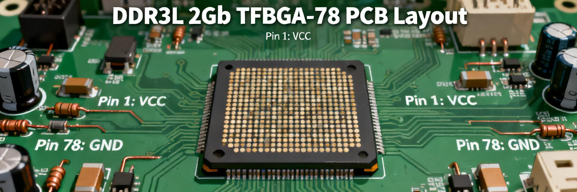
Point: The part is a 2Gb device organized as 256M x 8 in a 78-ball TFBGA footprint. Evidence: datasheet tables specify 256M x 8 array and TFBGA-78 package with standard ball mapping and power/ground islands. Explanation: designers must map the 256M x 8 banks to system address/data buses, account for bank addressing in the memory controller, and accommodate BGA escape routes in PCB layout for power and GND vias.
Performance snapshot: speed, voltage, temperature
Point: Expect DDR3L performance with up to ~1866 Mbps data rates and 1.35V nominal operation. Evidence: timing bins in the datasheet list max data rates and AC timing for listed speed grades, and DC specs show VDD/VDDQ ranges centered at 1.35V. Explanation: choose the speed grade that matches controller timing; for automotive/industrial grades confirm the expanded temperature window and prioritize parts rated for the required operating range.
| Parameter | Typical Value | Design Note |
|---|---|---|
| Density & Organization | 2Gb (256M x 8) | Map to byte-wide DQ bus |
| Package | TFBGA-78 | Plan BGA escape & assembly |
| Voltage | 1.35V (DDR3L) | Power-seq & decoupling required |
| Speed | Up to ~1866 Mbps | Select timing bin accordingly |
2: Electrical Characteristics & Timing Parameters (data analysis)
Core electrical specs & power envelopes
Point: VDD and VDDQ tolerances drive power budgeting and decoupling strategy. Evidence: datasheet DC tables give VDD/VDDQ ranges, standby/active currents, and recommended decoupling locations. Explanation: use multiple local decoupling caps by value (e.g., 0.1µF, 1µF) adjacent to VDD/VDDQ balls, budget peak active current for thermal design, and verify margins with voltage margining tests in the lab.
Timing table breakdown & interpreting tCL/tRCD/tRP
Point: CAS latency (tCL), tRCD, and tRP determine command-to-data timing and overall throughput. Evidence: AC timing tables list these parameters per speed bin and specify cycle counts and ns values. Explanation: read timing rows for each frequency, convert cycles to ns at the target data rate, and trade lower latency against timing margin—choose conservative timings for automotive-grade systems to prioritize reliability.
3: Interface, Signals & Packaging Details (data analysis)
Pinout / ball map and recommended footprint
Point: The TFBGA-78 ball map defines power, ground, address/command, and DQ banks that drive footprint decisions. Evidence: package diagrams in the datasheet show clustered power/ground balls and segregated command/address pins. Explanation: implement power islands with multiple vias, place bulk and high-frequency decoupling close to relevant balls, and respect recommended keepouts for temperature uniformity and assembly yield.
Signal timing, routing & termination best practices
Point: Address/command nets and DQ routing require different treatments for SI. Evidence: AC diagrams and recommended routing notes in the datasheet highlight CA bus constraints and DQ length-matching. Explanation: keep CA traces short and matched where required, apply per-byte DQ length matching within specified skew budgets, and use on-die termination/RT termination per vendor guidance to avoid reflections and setup/hold violations.
4: Thermal, Reliability & Qualification Notes (method guide)
Operating/Storage temperature and derating guidance
Point: Device temperature ratings inform derating and cooling strategies for long-term reliability. Evidence: datasheet lists operating and storage temperature windows and absolute maximums. Explanation: design for worst-case junction temperature, add thermal vias under the BGA, monitor board hotspots during validation, and apply derating curves (voltage/current) to ensure margin under elevated ambient conditions.
Reliability metrics and relevant compliance points
Point: MTBF indicators, retention, and endurance notes guide validation scope. Evidence: datasheet reliability notes and grade-specific statements describe expected behavior under stress. Explanation: perform environmental stress tests (temperature cycling, humidity), retention checks, and accelerate aging where needed; for automotive use, expand test matrices to include extended thermal and vibration profiles.
5: Design Integration & Validation Checklist (method guide)
Schematic & power-sequencing checklist
Point: Correct power sequencing and decoupling prevent latch-up and bad initialization. Evidence: datasheet power-up/power-down recommendations and recommended capacitor placements outline ordering and values. Explanation: enforce VDD/VDDQ sequencing in the power-plan, place bulk and high-frequency decoupling adjacent to appropriate balls, implement RESET/CK control pull resistors per guidelines, and verify sequencing with a controlled lab supply before firmware bring-up.
Validation tests to run before production
Point: Targeted tests validate electrical, thermal, and functional integration. Evidence: datasheet parameters define the ranges to verify for each test (AC timing, DC margins). Explanation: run read/write stress, voltage margining, temperature cycling, and IBIST/MBIST where supported; log deviations against datasheet limits and iterate layout or firmware timing to meet production acceptance criteria.
6: Troubleshooting, Cross-Reference & Sourcing Considerations (case/action)
Common failure modes and debug steps
Point: Timing violations, SI errors, and power-sequence faults are the most common integration failures. Evidence: oscilloscope captures compared to datasheet timing windows expose violations; power rail monitors reveal sequencing issues. Explanation: use a scope and logic analyzer to verify command-to-data timing, check VDD/VDDQ ramps against recommended profiles, and isolate signals with single-bit tests to locate marginal nets.
Cross-reference rules & parts selection tips
Point: Replacement selection requires matching electrical, timing, and package attributes. Evidence: cross-reference guidance compares density, speed, voltage, and package pinout compatibility. Explanation: only consider drop-in replacements when density, speed grade, voltage, pinout, and temperature grade match; otherwise re-validate SI and timing or redesign the footprint to prevent functional regressions.
Summary (10–15% of article)
- NT5CC256M8JQ-EKA is a 2Gb (256M x 8) DDR3L device in a 78-ball TFBGA: prioritize BGA escape planning, localized decoupling, and correct bank/address mapping for reliable integration.
- Key electricals—1.35V nominal, clear VDD/VDDQ tolerances, and timing bins—must be translated into power-sequencing, decoupling, and timing margin strategies referenced from the datasheet.
- Validation checklist: schematic power order, IBIST/MBIST or read/write stress, voltage margining, and thermal cycling are essential before production; consult the full datasheet tables for pin-exact details.
Frequently Asked Questions
How should engineers interpret the electrical specs in the datasheet?
Point: Electrical specs set the design envelope; evidence: DC tables list VDD ranges, currents, and recommended decoupling values. Explanation: designers should convert those numbers into a power budget, place targeted decoupling next to the BGA balls, and plan thermal margins, then verify with lab measurements against the datasheet limits.
What are the fastest checks to catch timing-related issues on the bench?
Point: Quick bench checks reveal most timing faults; evidence: scope traces compared to AC timing windows show setup/hold violations and skew. Explanation: capture CK-to-DQ timing, verify CA bus propagation, and perform length-matching audits—adjust controller timing or layout if traces violate datasheet-specified skew budgets.
Which validation tests are critical to qualify the memory on a new board?
Point: A focused test suite ensures robustness; evidence: datasheet limits guide each test’s pass/fail criteria. Explanation: run read/write stress, voltage margining, temperature cycling, and functional IBIST/MBIST where available—log results vs. datasheet values and iterate hardware or firmware until margins meet production requirements.
Can the 1.35V DDR3L NT5CC256M8JQ-EKA operate directly under legacy 1.5V DDR3 rails?
Point: While DDR3L standard specifies backward compatibility with 1.5V systems, powering an automotive-grade device at 1.5V increases active power consumption and thermal dissipation. Explanation: engineers must verify device junction temperatures and update power budgeting when operating outside nominal 1.35V rails.