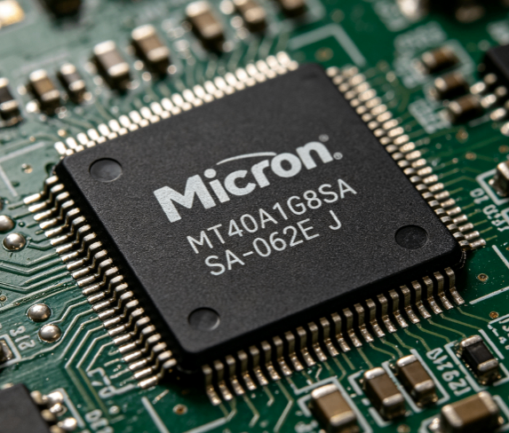
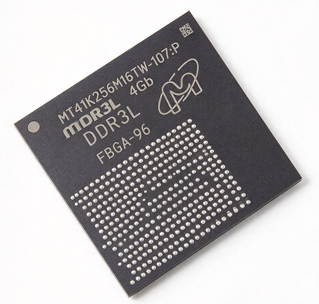
NT5TU32M16EG-AC Complete Datasheet, Pinout and Specifications
ThisNT5TU32M16EG-ACis a 512‑Mb DDR2 DRAM, featuring a 32M×16 memory organization, with a core supply voltage of 1.8 V and a typical signal rate of approximately 800 Mbps (400 MHz clock frequency). It is packaged in an 84-ball BGA. These specifications are particularly important for traditional and embedded DDR2 designs, where storage density, low voltage, and package size often determine board reusability and controller compatibility. This document serves as a practical reference, summarizing key points from the datasheet, pinout guidance, PCB/layout recommendations, and real-world troubleshooting methods to assist engineers in integratingNT5TU32M16EG-ACand citing the DDR2 datasheet for precise values.
Quick Overview and Key Specifications (Background)

Introduction to NT5TU32M16EG-AC — Brief Facts
Key points: This device is a 512-Mb (32M x 16) DDR2 memory chip, packaged in an 84-ball BGA package, suitable for commercial-grade applications. Evidence: The device is rated at VCC = 1.8 V, supports interface data rates up to approximately 800 Mbps, and features a standard DQ/DQS group selection with an 84-ball package. Explanation: This combination is primarily targeted at cost-sensitive embedded systems, traditional router boards, and industrial controllers—applications where DDR2 timing requirements and the BGA84 package size align well with existing circuit board designs and controller IPs.
When and why to choose this device
Key points: SelectionNT5TU32M16EG-ACSuitable for scenarios involving socket upgrades or when BOM costs are constrained and DDR2 is required. Evidence: Typical applications include embedded controllers and legacy platforms that rely on 1.8 V DDR2 signals and moderate bandwidth. Note: Before selecting a component, confirm whether the controller supports DDR2 voltage, CAS/timing options, and physical package constraints; also verify footprint dimensions, thermal paths, and I/O voltage tolerances on your PCB checklist.
Electrical Characteristics and Timing Summary (Data Analysis)
| Parameter Group | Nominal Value | Design Recommendations |
|---|---|---|
| Core Voltage (VCC/VDDQ) | 1.8 V ± 0.1 V | Place a 0.1 µF decoupling capacitor as close as possible to the solder balls. |
| Reference Voltage (VREF) | 0.49 × VDDQ to 0.51 × VDDQ | Avoid noise interference; maintain a minimum clearance of 15 mils between traces and signal paths. |
| Transmission Bandwidth | Up to 800 Mbps (clock frequency of 400 MHz) | Strictly adheres to differential trace routing constraints (100-ohm differential). |
| Dynamic refresh cycle | 8,192 cycles / 64 milliseconds (with a period of 7.8 microseconds) | Verify that the controller's automatic refresh interval matches the target junction temperature. |
Key electrical specifications to be extracted from the datasheet
Key points: Extract DC parameters—VCC, target values for VTT/VREF, input/output thresholds, and standby current—from the datasheet to design decoupling capacitors and power sequencing. Basis: The recommended operating ranges and Icc/Isb values in the datasheet determine the selection of decoupling capacitor arrays and the tolerance of power rails. Explanation: Place a 0.1 µF ceramic capacitor near the VCC pin, and configure larger 10 µF bulk capacitors on the power rails; allow a ±5% tolerance for power rails, and design VREF according to specifications to ensure reliable termination matching and reference stability.
Timing Parameters and Their Impact on Performance
Key points: Critical timing parameters include tCK (clock period), CAS latency options, tRCD, tRP, and tRAS; these parameters determine actual latency and throughput. Evidence: At a 400 MHz clock frequency, there is a significant difference in effective read latency and sustained bandwidth between CAS‑3 and CAS‑5 settings. Explanation: Effective bandwidth is calculated by considering the transfer rate (800 Mbps) and the CAS cycle; lower CAS can improve random access latency but may limit the maximum stable frequency—please match the controller timing table with the device timing table in the DDR2 datasheet.
Pinout and Package Details (Methodology Guide—Focusing on Pinout)
PBGA/VFBGA-84 Pinout Diagram and How to Read It
Key Points: The pin arrangement of the BGA84 groups power/ground, address/command, and DQ/DQS signals into separate areas; special attention should be paid to the VREF and DQS pins. Basis: According to the ball map and naming conventions in the datasheet, Vcc/Vss form clusters, DQ is divided into multiple groups, and the Vref balls are positioned adjacent to the DQ group to ensure stable reference voltage. Note: When reading, clearly identify the boundaries of each group, pay attention to the location near VREF, and match the ball names with the PCB netlist; use the term "pinout" in documentation and carefully verify the mask and ball numbers against the package drawing.
PCB Packaging, Routing, and Signal Grouping Techniques
Key points: For BGA84 DDR2 devices, pad layout accuracy and routing rules are critical. Evidence: Common failure modes stem from solder mask errors, misalignment of pad patterns, and poor via placement beneath the BGA. Explanation: Address/command signal traces should be kept as short as possible; the length of each DQ group must match its corresponding DQS clock pair; VREF signals should use low-impedance return path routing, with decoupling capacitors placed within 1–2 mm of the power ball grid; additionally, avoid using thermal isolation structures that could hinder solder reflow quality.
System Integration: Considerations (methods and measures) for power, timing, signal integrity, and thermal management
Power sequencing, decoupling, and reference design techniques
Key points: Proper power sequencing and decoupling can prevent latch-up phenomena and initialization anomalies. Evidence: Timing recommendations in datasheets typically require the core VCC to stabilize before VTT/VREF, and impose controlled rise times on I/O supply rails. Explanation: A sequence should be used where VCC is powered up first, followed by VDDQ, within the VREF tolerance range; meanwhile, distributed decoupling (0.01–0.1 µF ceramic capacitors paired with 4.7–10 µF bulk capacitors) should be employed near the package to control supply rail impedance during switching events.
Signal Integrity, Termination, and Thermal Management Guidelines
Key points: DQS termination and routing determine eye diagram quality and margin. Rationale: Series termination resistors, on-chip termination settings, and controlled-impedance traces are all listed as standard signal integrity mitigation measures. Explanation: Use small-value series resistors (5–22 Ω) at the DQ/DQS source to reduce reflections, match the length of each byte channel's DQ/DQS within approximately 100 ps, and ensure that the thermal conduction path from the BGA to the PCB is sufficient to support operation across commercial temperature ranges, thereby avoiding timing drift caused by temperature variations.
Integrated Checklist, Troubleshooting, and Alternatives (Cases + Mitigation Measures)
Pre-Production Checklist and Validation Testing
Key points: A streamlined pre-production process can accelerate product launch. Evidence: Effective verification items include pad layout validation, continuity testing, power rail verification, initialization, and basic read/write vector testing. Explanation: Before first power-up, verify pad patterns and network connections, confirm VCC/VDDQ/VREF voltages, use an oscilloscope to capture DQ/DQS alignment during controller initialization, and run address/command stress tests as well as long-term hold tests to validate system stability.
Common failure modes and quick troubleshooting methods; replace the reference
Key points: Faults typically stem from power sequencing, VREF bias errors, signal integrity issues, or soldering defects. Evidence includes training failures, frequent ECC or CRC errors, and poor eye diagram quality. Explanation: These can be improved by checking the timing sequence, measuring VREF tolerance, adding series resistors or adjusting drive strength, and inspecting the reflow process profile. For replacement components, verify density, timing, and pin compatibility at both the pad and timing table levels before cross-comparing alternative options.
Summary (Conclusion + Call to Action)
- ThisNT5TU32M16EG-ACis a 512‑Mb DDR2 (32M×16) chip in a BGA84 package, suitable for traditional embedded designs; please refer to the DDR2 datasheet for accurate electrical and timing specifications before integration.
- Key integration points to understand: strict power sequencing, local decoupling, VREF accuracy, and DQ/DQS length matching to meet signal integrity and training requirements.
- Startup steps: confirm package dimensions, verify power rails, use an oscilloscope to capture DQ/DQS signals, and run stress read/write test vectors before mass production.
Frequently Asked Questions
WhetherNT5TU32M16EG-ACIs it pin-compatible with other 84-ball DDR2 devices?
Pin compatibility varies by manufacturer; although the BGA84 package size is fairly standard, pin functions (such as VREF location, bank grouping) and ball map naming may differ. Be sure to compare.NT5TU32M16EG-ACBefore considering a candidate device as a direct replacement, please provide package drawings and ball grid maps, verify the layout of VREF and VTT, and confirm that the timing tables meet the controller's requirements.
What key parameters should be checked during design review?NT5TU32M16EG-ACWhat content is included in the DDR2 datasheet?
Key parameters include VCC/VDDQ tolerance, Icc/standby current, recommended VREF, tCK range, CAS latency options, tRCD/tRP/tRAS, and recommended decoupling schemes. Please cross-check these parameters against the system power budget, memory controller timing table, and thermal limits to ensure that the device can operate reliably on the target platform.
How to capture DQ/DQS alignment issues for ease ofNT5TU32M16EG-ACverification?
During training sequences, use a high-bandwidth oscilloscope and probe to measure representative DQ signals and their corresponding DQS clock signals; capture the eye diagram, measure setup/hold margins, and record skew between channels. If alignment fails, iteratively optimize by adjusting series resistor values, trace lengths, and drive strength or training parameters until the eye diagram meets the margin specifications outlined in the DDR2 datasheet.
For this BGA84 interface, what are the recommended layout and trace-matching targets?
The trace length for each group of 8-bit DQ signals must match the trace length of its corresponding DQS/UDQS clock signal, with a tolerance of ±100 picoseconds (approximately equivalent to 15 mm on a standard FR4 substrate). The ground reference plane beneath these traces must be continuous to ensure a clean 50-ohm single-ended / 100-ohm differential impedance path.