NT5TU32M16EG: DDR2 512Mb Specification and Pin Configuration Quick Report
1 — NT5TU32M16EG: Device Overview and Key Features
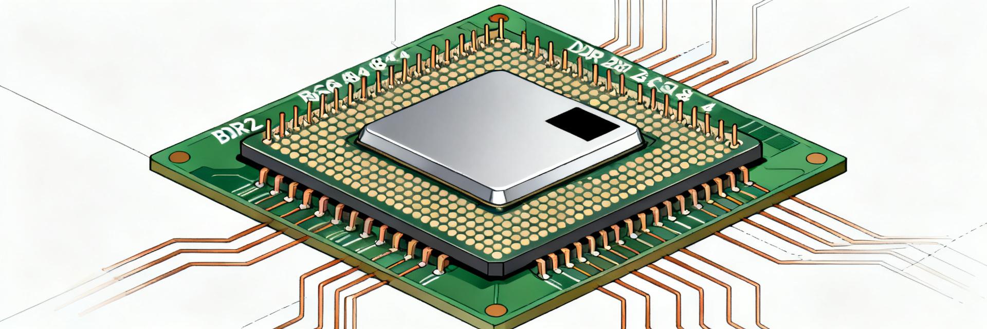
ThisNT5TU32M16EG-BEis designated as a standard DDR2, 512Mb high-speed SDRAM, configured in a single-row arrangement. Its core and interfaces both operate within a common 1.8V power domain, effectively reducing heat and power consumption. This IC is packaged in a standard BGA84 package, ensuring safe and reliable performance across traditional and current embedded workloads within commercial or industrial temperature ranges.
Key Parameters
| Parameter | Value |
|---|---|
| Density | 512Mb |
| Organization | 32M x 16 |
| I/O width | x16 |
| Nominal Vcc / Vddq | 1.8V ± 0.1V |
| Common speed grades | DDR2-400 / DDR2-533 / DDR2-667 |
| Package size | BGA, 84 solder balls (BGA84) |
2 — Electrical and Performance Breakdown (DDR2 512Mb)
The 32M x 16 architecture utilizes 32 million addressable locations, with each location storing 16 bits of data, thereby achieving 512 Mb of non-volatile storage. Bus transfers occur simultaneously on both edges of the clock signal (double data rate), enabling a maximum transfer rate of up to 667 Mbps per pin. The operating voltage is strictly maintained at 1.8 V; thermal design margins must account for the self-refresh current baseline and dynamic switching spikes. It is recommended to install dedicated bypass decoupling capacitors to limit power supply voltage droops during synchronous I/O operations.
3 — Pin Arrangement and Physical Layout
To reduce inductive interference and crosstalk, critical address, control, and data pins are assigned to separate clusters. Ground and power terminals are centrally arranged within the ball grid array, forming a direct low-inductance return path. Ensure that trace lengths between matched DQ channels are consistent, and maintain symmetrical routing for differential DQS strobe signals.
To achieve high-reliability PCB manufacturing, standard package layouts require clear thermal vias beneath the matrix center, specific solder stencil gaps, and strict clearance spacing around active memory traces.
4 — Timing, Signals, and Functional Description
Accurate parameter initialization can prevent bus contention during system startup. Before adjusting the system speed settings, set conservative timing values in the host memory controller registers.
Timing Reference Guide
| Parameter | Typical Reference Value |
|---|---|
| tCK | ~2.5 nanoseconds (at DDR2-400 speed) |
| tCAS (tCL) | 3 to 5 cycles (depending on the speed grade) |
| tRCD / tRP | ≥ tCL cycles (see device datasheet) |
5 — Integrated Checklist and Troubleshooting
During debugging after high-speed PCB layout and assembly, please be sure to keep the following hardware integration requirements in mind:
- Place the decoupling capacitor network (a combination of 0.1 µF and 10 µF) as close as possible to its corresponding power supply pins.
- Ensure that the trace impedance target is closely aligned with the controller's internal on-die termination (ODT) value.
- Differential signal lines (such as CLK and DQS) should be designed with symmetrical length tolerances.
Frequently Asked Questions
What is the recommended pinout reference for the NT5TU32M16EG?
Please use the device pinout diagram in the datasheet as the authoritative source for ball pin assignment. The device documentation lists the function of each ball pin and provides recommended handling for unconnected or reserved pins. During schematic design, verify the controller pin assignments against the mapping in the datasheet to avoid wiring errors in the DQ/DQS groups and power domains.
How should designers verify the timing of the NT5TU32M16EG during the debugging phase?
The controller is programmed using conservative mode register values, and read/write operations are performed to verify timing. During the early verification stage, eye diagrams of DQS and CLK are captured, and stress tests are conducted at the target data rate. If the margin is narrow, parameters such as tCL, tRCD, and tRP can be relaxed, or routing and termination can be adjusted; incremental adjustments combined with oscilloscope checks are used to ultimately determine reliable settings.
For common NT5TU32M16EG integration failures, what quick troubleshooting methods are available?
When errors occur, first check the power rails, Vref levels, and DQS alignment. Many faults stem from improper Vref settings, insufficient decoupling, or DQS skew causing setup/hold time violations. Use a multimeter to verify Vdd/Vddq voltages, inspect the placement of decoupling capacitors, then use an oscilloscope to align DQS signal edges, adjusting trace lengths or on-board delay elements as needed.
What are the core operating voltage requirements for the NT5TU32M16EG architecture?
The memory core and I/O domains operate at a nominal 1.8V VDD/VDDQ power rail. To suppress transient currents during read/write operations and ensure power integrity, decoupling capacitors (0.1µF and 10µF) must be placed directly near the power pins.