NT6TL128M32BQ-G0 Datasheet Detailed Analysis: Specifications and Pin Configuration
In modern mobile and embedded designs, the choice of low-power mobile SDRAM directly impacts boot time, power budget, and sustained memory throughput. The NT6TL128M32BQ-G0 is a 4Gb mobile LPDDR2‑class device that operates at voltages below 1.2V and supports a peak data rate of approximately 1066 Mbps. This summary transforms the official datasheet into a practical guide for integration, testing, and layout. You will find concise explanations of which electrical and timing parameters are most critical, how pin assignments map to PCB nets, and common integration pitfalls that can prolong debugging cycles.
This in-depth analysis references tables from the datasheet and outlines practical checks to be performed during schematic review, PCB layout, and system startup. To ensure search relevance and help you directly map the guidance to your chosen device, the article begins by listing two specific device models (NT6TL128M32BQ-G0). The following sections categorize the device into background and specifications, electrical/timing constraints, pinout and package guidelines, initialization sequence, and a practical troubleshooting checklist.
1 Background and Key Specifications Overview (Background Introduction)
Quick Specification Overview (1)
Key Points: A concise summary of specifications to clarify architectural trade-offs. Basis: All key data below are extracted from tables in the device's datasheet. Explanation: Factors such as capacity, organization, package type, voltage levels, and transfer rates determine controller selection and PCB design limitations.
| Item | Value |
|---|---|
| Density | 4 Gbit |
| Organization | 128M × 32 |
| Package | 168-ball PoP / FBGA |
| VDD / VDDQ (nominal values) | ~1.2 V / 1.2 V (I/O) |
| Data rate | 800–1066 Mbps |
| Temperature range | −25°C to +85°C (typical commercial) |
| Standby/operating current | Typical IDD0/IDD1 parameters are listed in the data sheet summary. |
System impact: A 4Gb device in x32 mode can provide a wide DQ bus, reducing access cycles for high-bandwidth transfers, but it requires a controller that supports 32-bit channels and corresponding command/address timing. The PoP package simplifies stacking design, yet imposes strict requirements on height and thermal management. Please match the controller's I/O voltage tolerance with VDDQ and allow sufficient margin for voltage ramps during power sequencing.
Device model and part number description (1)
Key points: The model suffix indicates the speed grade or temperature grade. Basis: The model table in the datasheet lists commercial-grade and extended-grade options. Explanation: When checking device markings, please verify the suffix against the model table in the datasheet; differences in speed grades typically affect timing parameters, while temperature grades relate to derating design and PCB thermal management planning. Also, pay attention to any power limitations associated with specific models, as these will impact decoupling design and the determination of copper foil area.
2 Electrical Characteristics and Timing Depth Analysis (Data Analysis)
DC Electrical Parameters (1)
Key points: Under operating conditions below 1.2 V, DC margin and decoupling are critical. Basis: The datasheet tables clearly specify the recommended operating voltage and current ranges. Explanation: Please refer to the absolute maximum ratings, the suggested VDD and VDDQ power rails, and the summarized IDD operating modes (IDD0/IDD1/IDD2). Use multiple local decoupling capacitors near the VDD and VDDQ pins (e.g., 0.1 µF + 1 µF per power domain), place large-capacitance capacitors on the power rails, and ensure that the distance between the decoupling capacitors and the device pins remains within 2–3 mm. Monitor voltage margins during power-up, and apply thermal derating during startup to ensure adequate safety margins.
AC Timing and Performance (1)
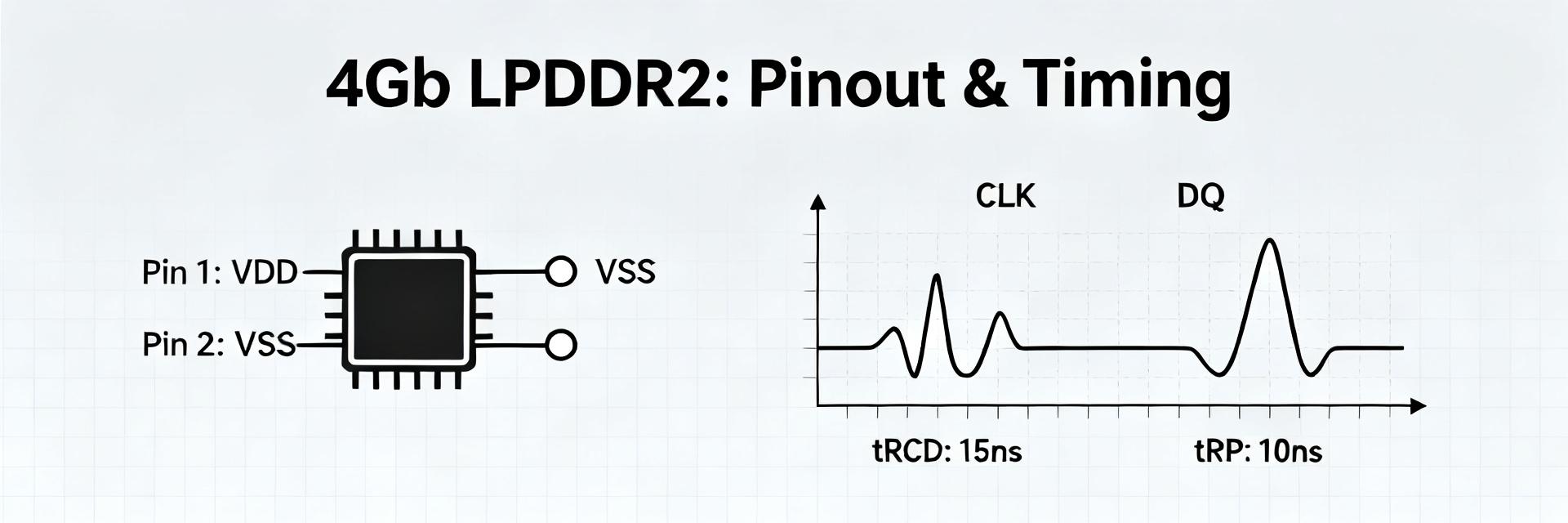
Key points: AC timing determines the controller's configuration and observable signals. Evidence: The datasheet's timing tables list tRCD, tRP, tRAS, tRC, CAS latency options, and the DQS timing window. Explanation: Configure clock ranges and CAS latencies according to supported data rates; verify tRCD/tRP/tRAS against the controller's default values. On the test bench, use an oscilloscope to check the DQS capture window and command-to-data timing—align DQS with the center of the data eye and confirm that the refresh interval meets requirements. The datasheet provides the timing budget that must be satisfied to ensure reliable operation.
3 Pin Arrangement and Package Details (Method Guide/Pin Configuration)
Ball Grid Array Diagram and Functional Grouping (1)
Key points: Group pins by function to simplify schematic net naming. Basis: The package table categorizes power, address/command, data, DQS, clock, and control pins separately. Explanation: Map pins to power (VDD, VDDQ, VSS), CA (command/address), DQ (data), DQS (data strobe), CK/CK# (clock differential pair), and control signals (RESET#, CKE). In the schematic, use net names such as VDD_CORE, VDD_IO, DQ[31:0], DQS[7:0], CA[12:0], CK0, CK0#, etc., to maintain consistency. Note special-purpose pins (e.g., test pins, NC) and, following the pinout guidelines in the datasheet, designate them as floating or test pins.
Considerations for Package and PCB Pads (1)
Key points: The pad layout and thermal management strategies of PoP are critical for assembly and reliability. Evidence: The datasheet recommends specific pad patterns and limits on reflow soldering process parameters. Explanation: Recommended pad patterns and solder mask openings should be used; unless filled, via-type pads should be avoided directly beneath BGA balls. For PoP stack-up designs, keep clearances and thermal vias near power balls to improve heat dissipation, but limit the number of vias in critical signal areas. During assembly, strictly follow the reflow profile specified in the datasheet, control the peak temperature, and minimize mechanical stress.
4 Initialization, Command Sequences, and Example Integration (Method Guide/Case Studies)
Power-Up/Power-Down and Reset Timing (1)
Key point: Proper power-rail sequencing prevents latch-up and functional failures. Basis: The datasheet specifies the sequence for applying VDD/VDDQ and the tPOR timing. Explanation: Raise the core supply VDD and the I/O supply VDDQ to their nominal levels at controlled rise/fall rates, wait until the minimum tPOR is met, then assert RESET# or apply the clock signal CK. Verify that each power rail has reached the correct voltage and maintains a low-impedance path; wait for the specified delay before the first valid access. During power-down, reverse the sequence and allow sufficient decay time to prevent charge trapping.
Example Controller Initialization and Calibration Procedure (1)
Key points: The firmware must program the mode registers and perform impedance calibration when applicable. Evidence: The datasheet demonstrates the MR settings and ZQ operation procedure. Explanation: After power-up and ensuring clock stability, program the mode registers for CAS latency and drive strength; if supported, perform ZQ/impedance calibration, enable auto-refresh, and verify low-power-related configurations. Checklist: Set the MR values, wait the specified nanoseconds/microseconds between commands, and confirm calibration completion by examining the DQS eye diagram. Use an oscilloscope probe to verify DQS alignment and the calibration-complete signal.
5 Integrated Practical Checklist and Troubleshooting Guide (Action Recommendations)
PCB Layout and Signal Integrity Checklist (1)
Key points: SI rules directly affect data integrity. Evidence: At data rates of 800–1066 Mbps, wide DQ buses require matched routing. Explanation: Implement controlled impedance traces for DQ/DQS/CK (typically 50Ω single-ended and 100Ω differential, depending on the situation), match DQ/DQS lengths within the specified skew budget, minimize vias along the data path, establish separate power planes between the core and I/O, and place decoupling capacitors close to device pins. Setting probe points near DQS and CK helps improve debugging convenience.
Common faults and diagnostic steps (1)
Key points: Typical faults usually have reproducible debugging procedures. Evidence: Common root causes include power sequencing, voltage errors, timing violations, and poor routing. Explanation: Reproduce the fault, verify DC power rails and power sequencing, check for clock presence and integrity, inspect DQS alignment and eye diagrams, and confirm refresh behavior. Use stress test modes (full-width write/read, continuous refresh load) to distinguish firmware from hardware issues, and prioritize fixes based on likelihood and cost.
Key Summary
- The NT6TL128M32BQ-G0 is a 4Gb LPDDR2-class device; during initial power-up, ensure that the VDD/VDDQ power rails are correct and properly decoupled to prevent "brown-in" or system instability.
- Pin grouping (power, CA, DQ, DQS, CK, control) helps simplify schematic naming and layout—be sure to match DQ/DQS and minimize the number of vias required for signal integrity.
- AC timing (tRCD/tRP/tRAS, CAS, DQS alignment) determines the controller settings; verify through oscilloscope testing and adhere to the timing budgets in the datasheet to ensure reliable operation.
Frequently Asked Questions about the NT6TL128M32BQ-G0 Integration
What are the key power sequencing steps for the NT6TL128M32BQ-G0?
Follow the sequence specified in the datasheet: raise VDD and VDDQ to their nominal values at controlled rise/fall rates, and wait for the specified tPOR time before applying RESET# or clock signals. Confirm voltage and current at each stage, and allow a minimum delay before the first memory access to avoid latch-up or undefined states.
How should DQS alignment and timing be verified on the test bench?
Use a high-speed oscilloscope and differential probes to capture DQS, DQ, and CK signals. Check whether DQS centers the data eye diagram and whether the sampling edges meet the setup/hold time margins. Verify timing against the tSU/tH windows specified in the datasheet, and perform eye diagram scans at the target data rate.
Which layout practices most often resolve intermittent memory errors?
Match the lengths of DQ and DQS within the specified skew range, use controlled impedance routing, minimize vias along critical data paths, provide dedicated power planes with targeted decoupling, and avoid crossing high-speed return current paths. These improvements typically address timing and signal integrity issues.
What are the typical voltage levels and temperature tolerances for NT6TL128M32BQ-G0?
The nominal operating voltage is 1.2V in both the VDD (core) and VDDQ (I/O) domains. The standard commercial temperature range is −25°C to +85°C. During hardware debugging, ensure that thermal conditions and voltage margins are thoroughly evaluated.
Summary: The NT6TL128M32BQ-G0 is a 4Gb mobile LPDDR2‑class device. Its reliable integration depends on strict adherence to the electrical and timing constraints specified in the datasheet, a carefully designed pinout and package footprint, and proper power sequencing. Please download the official datasheet PDF and verify the pin configuration and part specification table for the NT6TL128M32BQ-G0 during final layout review.