.geo-fragment, .geo-fragment *, .geo-fragment *::before, .geo-fragment *::after {
box-sizing: border-box;
}
.geo-fragment {
font-family: -apple-system, BlinkMacSystemFont, "Segoe UI", Roboto, Helvetica, Arial, sans-serif;
color: inherit;
line-height: 1.8;
max-width: 100%;
margin: 0 auto;
}
.geo-fragment h1 {
font-size: 36px;
font-weight: 800;
line-height: 1.25;
margin-top: 0;
margin-bottom: 28px;
color: inherit;
}
.geo-fragment h2 {
font-size: 26px;
font-weight: 700;
line-height: 1.3;
margin-top: 40px;
margin-bottom: 20px;
border-left: 5px solid currentColor;
padding-left: 12px;
color: inherit;
}
.geo-fragment h3 {
font-size: 20px;
font-weight: 600;
margin-top: 24px;
margin-bottom: 12px;
color: inherit;
}
.geo-fragment p {
font-size: 16px;
margin-bottom: 1.5em;
color: inherit;
opacity: 0.95;
}
.geo-fragment ul {
margin-bottom: 1.5em;
padding-left: 20px;
}
.geo-fragment li {
margin-bottom: 0.5em;
}
.geo-fragment table {
width: 100%;
border-collapse: collapse;
margin: 24px 0;
font-size: 14px;
animation: geoFadeIn 0.8s ease-out forwards;
}
.geo-fragment thead th {
font-weight: 600;
text-align: left;
padding: 12px;
border-bottom: 2px solid currentColor;
}
.geo-fragment tbody tr {
border-bottom: 1px solid currentColor;
transition: background-color 0.2s ease;
}
.geo-fragment tbody tr:hover {
background-color: rgba(128, 128, 128, 0.08);
}
.geo-fragment tbody td {
padding: 12px;
}
.geo-fragment svg {
display: block;
margin: 32px auto;
max-width: 100%;
height: auto;
animation: geoFadeIn 0.8s ease-out forwards;
}
.geo-fragment details {
border-bottom: 1px solid currentColor;
padding: 16px 0;
animation: geoFadeIn 0.5s ease-out forwards;
}
.geo-fragment summary {
list-style: none;
outline: none;
cursor: pointer;
font-weight: 600;
font-size: 16px;
display: flex;
justify-content: space-between;
align-items: center;
}
.geo-fragment summary::-webkit-details-marker {
display: none;
}
.geo-fragment summary::after {
content: "+";
font-size: 20px;
font-weight: 400;
transition: transform 0.2s ease;
}
.geo-fragment details[open] summary::after {
content: "−";
}
.geo-fragment .faq-answer {
padding-top: 12px;
font-size: 15px;
}
.geo-fragment .img-container {
margin: 24px 0;
max-width: 100%;
}
.geo-fragment .img-container img {
width: 100%;
height: auto;
display: block;
}
@keyframes geoFadeIn {
from {
opacity: 0;
transform: translateY(10px);
}
to {
opacity: 1;
transform: translateY(0);
}
}
{
"@context": "https://schema.org",
"@graph": [
{
"@type": "TechArticle",
"@id": "https://example.com/article/mt53d1024m32d4dt-report#article",
"headline": "LPDDR4 32Gb MT53D1024M32D4DT: Performance Report & Deep Dive",
"description": "Comprehensive engineering evaluation of the MT53D1024M32D4DT 32Gb LPDDR4 memory device, highlighting peak vs sustained bandwidth, signal integrity, and system validation.",
"articleBody": "The MT53D1024M32D4DT is a 32Gb LPDDR4 device rated to 2133 MT/s with a x32 I/O. It achieves a peak bandwidth of ~8.53 GB/s per package under ultra-low core voltages (~0.6V). To fully convert these datasheet figures to sustained system performance, engineers must carefully manage PCB signal integrity, VREF training, and power delivery margins."
},
{
"@type": "Product",
"@id": "https://example.com/product/mt53d1024m32d4dt#product",
"name": "MT53D1024M32D4DT",
"description": "LPDDR4 SDRAM 32Gb (1G x 32) memory chip featuring low core operation voltage of 0.6V and speeds up to 2133 MT/s.",
"offers": {
"@type": "Offer",
"priceCurrency": "USD",
"price": "45.50",
"availability": "https://schema.org/InStock"
},
"review": {
"@type": "Review",
"reviewRating": {
"@type": "Rating",
"ratingValue": "5",
"bestRating": "5"
},
"author": {
"@type": "Organization",
"name": "FAE Team"
}
}
},
{
"@type": "FAQPage",
"@id": "https://example.com/faq/mt53d1024m32d4dt#faq",
"mainEntity": [
{
"@type": "Question",
"name": "What is the theoretical vs. realistic sustained bandwidth of the MT53D1024M32D4DT?",
"acceptedAnswer": {
"@type": "Answer",
"text": "The theoretical peak bandwidth at 2133 MT/s with a x32 bus is approximately 8.53 GB/s. In real-world operation, due to command overhead, refresh cycles, and controller arbitration, designers should expect sustained sequential bandwidth of 60% to 80% of peak (approx. 5.1 to 6.8 GB/s), while random small-block workloads may drop below 30% to 40%."
}
},
{
"@type": "Question",
"name": "What typical LPDDR4 latency should designers expect and how does it change with frequency?",
"acceptedAnswer": {
"@type": "Answer",
"text": "Observed LPDDR4 latency varies with timing settings and operating frequency. Convert cycles to nanoseconds using the transfer period (1/MT/s); increasing frequency shortens cycle time but can increase dynamic power. Designers should measure read/write latency across training points and report median and tail percentiles to capture controller-dependent behavior."
}
},
{
"@type": "Question",
"name": "How does a 32Gb device impact PCB layout compared with lower-density parts?",
"acceptedAnswer": {
"@type": "Answer",
"text": "Higher-density 32Gb packages often increase ball count and require tighter escape routing, making controlled impedance and trace matching more challenging. Place the device close to the controller, minimize stub lengths, and prioritize via strategy and decoupling placement to preserve signal integrity and training margin."
}
},
{
"@type": "Question",
"name": "What validation steps are essential before qualifying MT53D1024M32D4DT in production systems?",
"acceptedAnswer": {
"@type": "Answer",
"text": "Essential validation includes interoperability testing with target controllers, burn-in and stress testing across worst-case temperatures and voltages, VREF calibration and eye diagram margining, and statistical sample runs to verify error-free operation. Document part markings and revision tracking, and confirm long-term availability before final procurement."
}
}
]
}
]
}
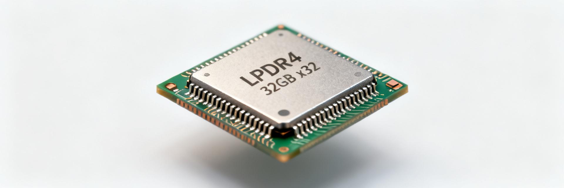
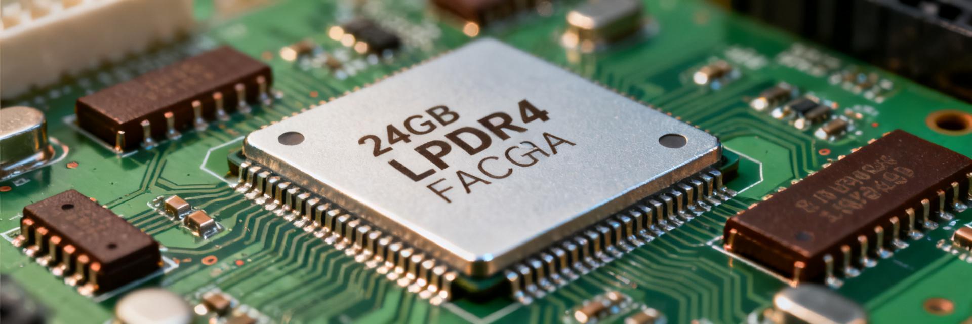
The MT53D1024M32D4DT is a 32Gb LPDDR4 device rated to 2133 MT/s with a x32 I/O (4 bytes/transfer) and ultra-low-voltage core operation (~0.6 V). Translating the headline numbers: 2133 MT/s × 4 bytes = ~8.53 GB/s peak per device, which sets an upper system-bound for a single x32 LPDDR4 package. This report verifies real-world bandwidth, latency, power, and integration trade-offs designers will face when bringing such a device into mobile or embedded platforms. It also prescribes reproducible benchmark methodology and practical PCB, power, and firmware checks so system teams can confirm that datasheet peak figures convert into predictable sustained throughput in their designs.
1 — Background: LPDDR4 32Gb Architecture & Key Specifications
What "32Gb" and x32 mean for capacity and bus width
Point: "32Gb" denotes gigabits of raw DRAM storage; x32 indicates a thirty-two-bit wide data bus, or four bytes per transfer. Evidence: 32 gigabits equals 4 gigabytes of raw capacity per die; a x32 device delivers four bytes per cycle, so effective peak bandwidth follows transfers×4. Explanation: For designers, a single 32Gb LPDDR4 device typically appears as 4 GB of addressable memory; multi-rank or multi-device assemblies increase capacity or parallelism. Bus width choices (x16 vs x32) affect controller channel mapping, PCB pin count, and achievable peak per-channel throughput.
Physical package, voltage rails, and thermal/operating ranges
Point: LPDDR4 packages for 32Gb parts are typically small FBGA/QDP with high ball counts and tight footprints; they require multiple low-voltage rails. Evidence: Typical rails include VDD (core), VDDQ (I/O), and a pump or VPP rail where applicable; core voltages approach 0.6 V while I/O commonly sits near 1.05–1.2 V. Explanation: Designers must budget PCB real estate for dense BGA escape routing, place decoupling close to balls, and select power supplies that meet sequencing and transient specs; operating temperature windows differ for consumer versus industrial variants and affect margin requirements.
Parameter
Specification Details
Target Value / Range
Density / Capacity
Total Addressable Capacity
32Gb (4 Gigabytes)
Bus Width
Data Interface Configuration
x32 (Dual-Channel Architecture)
Data Rate
Maximum Rated Operational Frequency
2133 MT/s (DDR clock: 1066 MHz)
Peak Bandwidth
Theoretical Interface Limit
~8.53 GB/s per device
Core Voltage (VDD2)
Ultra-Low Core Operation Voltage
~0.6 V (Nominal)
I/O Voltage (VDDQ)
Low-Voltage Swing Interface
~1.1 V / 1.2 V
Memory Controller
CA [5:0] (Control Bus)
DQ [31:0] (Bi-dir Data Bus - 4 Bytes)
CK_t / CK_c (Diff. Clock)
MT53D1024M32
32Gb LPDDR4
VDD2: 0.6V | VDDQ: 1.1V
2 — Performance Data Deep-Dive: Bandwidth, Latency & Power
Calculating theoretical throughput and realistic effective bandwidth
Point: Theoretical peak = data rate × bytes per transfer; at 2133 MT/s and x32 that equals ~8.53 GB/s. Evidence: Translating MT/s to bytes/s is straightforward, but effective throughput is reduced by command overhead, refresh, and bus utilization patterns. Explanation: Expect sustained bandwidth in practice to be a fraction of peak—typical sustained ranges for streaming sequential reads are often 60–80% of peak (≈5.1–6.8 GB/s) while random small-block workloads can fall below 30–40% depending on controller efficiency. Use sequential large-block, mixed RW, and random small-block tests to expose those limits.
Latency, timing parameters (CAS, tRCD, tRP) and power characterization
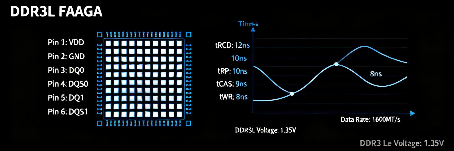
Point: Timing parameters expressed in cycles map to absolute latency via the device clock period; power has distinct active, standby, and IO components. Evidence: Calculate t(ns) = cycles × (1/MT/s) and measure idle vs active currents with a precision power meter while exercising read/write patterns. Explanation: Higher frequency reduces cycle time and can lower cycle-to-nanosecond conversion but may increase dynamic power. Measure average power under realistic workloads and derive power-per-GB by dividing measured watts by sustained GB/s to compare operating points and trade-offs.
3 — Benchmark Methodology: How to Measure MT53D1024M32D4DT Accurately
Testbench, tooling and test vectors
Point: Accurate measurement requires a controller or FPGA capable of LPDDR4 training and a precision power/measurement chain. Evidence: Use an FPGA with a validated DDR PHY or a controller evaluation board, a high-speed scope for eye and timing, and a power meter with sub-10 mW resolution plus logic capture for command traces. Explanation: Recommended workloads include sequential large-block streaming, random small-block IOPS, mixed RW at several ratios, and captured real-world traces (multimedia decode, packet buffers) so results map to target applications.
Reproducibility, configuration, and reporting standards
Point: Reproducible reports require consistent training, sample size, and statistical reporting. Evidence: Run multiple warm-up iterations, perform JEDEC-like training steps, and capture median and 95th-percentile metrics across samples and temperatures. Explanation: Report clock rate, voltage rails, temperature, firmware/timing settings, and error counts; include sample size and run-to-run variance so readers can assess confidence and reproduce the methodology in their labs.
4 — Integration Considerations for System Designers
PCB layout, signal integrity and routing best practices
Point: Layout dominates whether a 32Gb device hits its throughput and training window. Evidence: Tight trace length matching, controlled impedance, minimized stubs, and optimal placement relative to controller reduce reflections and timing skew. Explanation: Use dedicated DDR routing layers, match fly-by topologies where required, place decoupling capacitors adjacent to power balls, and follow recommended via strategies; poor SI often manifests as failed training or marginal eye diagrams that limit usable data rate.
Power delivery, thermal management and firmware/timing tuning
Point: Stable low-voltage rails and thermal headroom are prerequisites for rated performance. Evidence: Implement bulk and local decoupling, enforce power-sequence order, and monitor VREF calibration during bring-up. Explanation: During firmware tuning, adjust timing margins, retrain at target temperatures, and use thermal derating to preserve reliability; a bring-up checklist should include VREF calibration, eye checks, and margin testing under worst-case voltage and temperature.
5 — Use Cases, Trade-offs & Procurement/Validation Checklist
Target applications and system-level trade-offs
Point: A 32Gb LPDDR4 x32 device targets high-bandwidth mobile and embedded systems that need 4 GB per device at relatively low power. Evidence: Suitable applications include image/vision pipelines, network packet buffers, and accelerators that favor single-channel high-throughput memory versus costlier multi-channel solutions. Explanation: Evaluate cost vs capacity, single-die vs multi-die packages, and whether moving to higher-density LPDDR or multiple channels yields better system throughput-per-watt for your workload.
Procurement, sample validation and lifecycle considerations
Point: Procurement and validation must confirm markings, revisions, and sample adequacy before production. Evidence: Order engineering samples, track part revisions, perform burn-in and stress tests, and validate interoperability with target controllers across temperature. Explanation: A practical checklist should include verifying part marking, sample quantity for statistical confidence, burn-in plans, interoperability matrix, and long-term supply assurances to avoid late-design surprises.
Summary
In brief, a 32Gb LPDDR4 x32 device operating at 2133 MT/s yields ~8.53 GB/s peak per device, but practical results depend on controller efficiency, layout, timing, and power design. Use the benchmark methodology and integration checklist above to translate datasheet figures into reproducible system metrics and to validate margin across temperature and voltage. Below are concise takeaways and practical next steps for engineering teams.
Peak vs sustained: Expect ~8.53 GB/s peak from LPDDR4 x32 at 2133 MT/s, with sustained sequential throughput typically 60–80% of peak; plan system buffers and controller arbitration accordingly.
Integration matters: PCB routing, decoupling, and power sequencing strongly influence training success and latency; treat layout and PDN as first-order performance parameters for 32Gb devices.
Measurement & validation: Use controlled testbenches, multiple runs, and percentile reporting; validate under worst-case temperature/voltage to ensure MT53D1024M32D4DT-class parts meet system SLAs.
Frequently Asked Questions
What is the theoretical vs. realistic sustained bandwidth of the MT53D1024M32D4DT?
The theoretical peak bandwidth at 2133 MT/s with a x32 bus is approximately 8.53 GB/s. In real-world operation, due to command overhead, refresh cycles, and controller arbitration, designers should expect sustained sequential bandwidth of 60% to 80% of peak (approx. 5.1 to 6.8 GB/s), while random small-block workloads may drop below 30% to 40%.
What typical LPDDR4 latency should designers expect and how does it change with frequency?
Observed LPDDR4 latency varies with timing settings and operating frequency. Convert cycles to nanoseconds using the transfer period (1/MT/s); increasing frequency shortens cycle time but can increase dynamic power. Designers should measure read/write latency across training points and report median and tail percentiles to capture controller-dependent behavior.
How does a 32Gb device impact PCB layout compared with lower-density parts?
Higher-density 32Gb packages often increase ball count and require tighter escape routing, making controlled impedance and trace matching more challenging. Place the device close to the controller, minimize stub lengths, and prioritize via strategy and decoupling placement to preserve signal integrity and training margin.
What validation steps are essential before qualifying MT53D1024M32D4DT in production systems?
Essential validation includes interoperability testing with target controllers, burn-in and stress testing across worst-case temperatures and voltages, VREF calibration and eye diagram margining, and statistical sample runs to verify error-free operation. Document part markings and revision tracking, and confirm long-term availability before final procurement.