NL0333DCAE1S-ES Datasheet Deep Dive: Key Specs & Pinout
Technical analysis of precision low-power, zero-drift operational amplifiers for sensor front-ends.
The NL0333DCAE1S-ES datasheet contains the electrical boundaries and layout notes that determine success when using a precision low-power, zero-drift operational amplifier in sensor front-ends and battery-powered nodes. This introduction synthesizes the datasheet’s headline numbers—supply range, offset and drift, quiescent current, output swing and stability guidance—and frames them as immediate checklist items for schematic and PCB decisions. Engineers will find concise guidance to verify pinout and footprint constraints and to adopt layout and test practices that preserve the part’s precision in production.
Reading the datasheet with a focus on manufacturability and testability reduces re-spins: identify absolute maximums early, confirm the pinout and exposed pad behavior, and translate typical-characteristic graphs into pass/fail bench limits. The remainder of this deep dive distills the datasheet into actionable rules, measurement points and layout prescriptions for reliable designs using this device.
1 — Product context: what NL0333DCAE1S-ES is and where it fits (Background)
The NL0333DCAE1S-ES is a precision, low-power zero-drift op amp intended for sensing and low-drift signal chains where long-term stability and minimal offset are priorities. In system contexts such as thermopile sensor interfaces, battery-powered data loggers and low-drift instrumentation, the device’s low offset and low quiescent current reduce calibration overhead while extending battery life.
1.1 — Functional description & target applications
Functionally, the device operates as a rail-friendly precision amplifier optimized for DC accuracy rather than high-speed gain. Typical applications include sensor amplification, long-time-constant filters and single-supply instrumentation where offset and drift dominate measurement error. Engineers should weigh the device when system constraints demand sub-millivolt offset drift, tight long-term stability, and low idle currents that preserve battery life in always-on monitors.
1.2 — Competitive role & selection rationale
Selection involves a trade-off matrix: precision versus power and offset drift versus BOM cost. Key decision factors include required offset and drift, allowed supply current, package and PCB area, and output swing against expected load. Quick checklist: (1) choose this part when offset/drift budgets are tight; (2) validate quiescent current against power budget; (3) confirm package/pinout fits the board’s thermal and grounding plan.
2 — Key electrical specifications: datasheet numbers you must know (Data analysis)
Engineers must extract absolute maximums and recommended operating conditions first, then the continuous electrical characteristics that affect accuracy. The NL0333DCAE1S-ES datasheet outlines both limit values and typical-performance curves—those figures drive bench-test conditions and temperature-based deratings.
2.1 — Absolute maximums & recommended operating conditions
Critical limits to record: minimum and maximum supply voltages, input common-mode boundaries, maximum differential input, junction and ambient temperature ranges, and device power dissipation. Exceeding supply or input limits can cause latch-up or permanent offset shifts; thermal overstress reduces long-term stability.
2.2 — Electrical characteristics & typical performance
| Parameter | Typical | Max / Notes |
|---|---|---|
| Supply range | See datasheet recommended range | Absolute max must not be exceeded |
| Input offset / drift | Low (µV-level typical) | Specifies max over temp |
| Quiescent current | Low µA range | Temperature-dependent |
| Output swing | Near rail (load-dependent) | Specify RL |
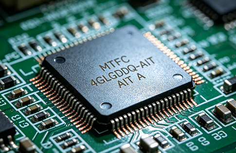
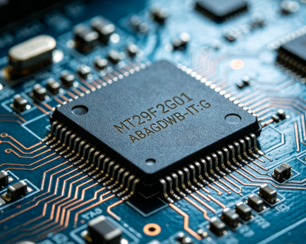
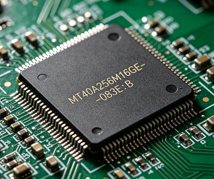
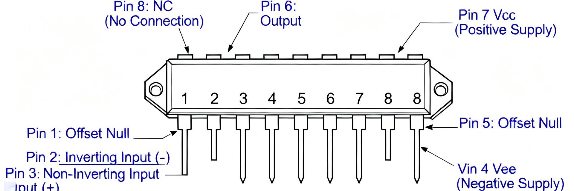
3 — Pinout, package & PCB footprint (Design-critical pinout)
Clear labeling of each pin is essential: supply rails, non-inverting and inverting inputs, outputs, and any NC or substrate pins must be annotated on the schematic and footprint. Note whether an exposed pad is present and whether the datasheet requires it to be tied to ground or to the substrate.
3.1 — Pinout diagram & pin descriptions
For each pin, document expected signal range and any special behavior: power pins (V+ and V– or ground), inputs (observe input common-mode), outputs (allow for load-dependent swing) and substrate/exposed pad (tie to ground per datasheet).
3.2 — Package dimensions, thermal pad & recommended land pattern
Read the mechanical drawing carefully: record package code, body dimensions, exposed pad footprint and recommended solder-land geometry and tolerances. For thermal and grounding practice, stitch the exposed pad to a ground plane with multiple vias.
4 — Application circuits and layout best practices (Method / how-to)
Canonical circuits demonstrate how to preserve accuracy: unity-gain buffers for impedance isolation, single-supply non-inverting amplifiers for sensor conditioning, and low-pass filters for anti-aliasing.
4.1 — Typical application circuits to include
Recommend three circuits: unity buffer for impedance matching, single-supply non-inverting sensor amplifier with R values sized to balance noise and bias currents, and a passive or active RC low-pass filter placed before ADC input.
4.2 — PCB layout, decoupling and stability tips
5 — Testing, validation & sourcing checklist (Actionable checklist)
Before production, compile a verification plan that includes electrical spot checks, thermal characterization and assembly validation.
5.1 — Recommended bench tests
- Quiescent current at nominal VCC
- Input offset & drift vs temperature
- Output swing into expected RL
- Noise spot checks (defined BW)
5.2 — Ordering & Compliance
- Confirm full part number suffix
- Verify package code & marking
- Check RoHS/lead-free status
- Verify tape/reel info
Summary
- Observe the NL0333DCAE1S-ES electrical limits: supply range, input common-mode and thermal ratings define safe operating space and must be validated on the board to protect precision performance.
- Pinout and footprint matter: correctly tie the exposed pad to ground, follow recommended land patterns, and verify pin markings to prevent assembly or thermal issues that degrade accuracy.
- Layout and test discipline preserve precision: close decoupling, guarded input routing, capacitance management and a clear bench verification plan ensure the datasheet performance translates to production.
Common questions and answers
What are the most critical datasheet limits for NL0333DCAE1S-ES?
The most critical limits are the recommended supply voltage range and absolute maximums, input common-mode boundaries, maximum input differential and thermal junction limits. Engineers should treat these as hard constraints in schematic and PCB design and verify them by measuring supply rails and junction temperatures under worst-case load during prototype testing.
How should engineers verify the NL0333DCAE1S-ES pinout and footprint on their PCB?
Cross-check the PCB land pattern with the mechanical drawing, confirm pad and exposed pad dimensions, and review pin-mode functions (power, inputs, outputs, NC). Perform a footprint verification on a 1:1 printed overlay, and inspect the first populated boards for solder quality and correct orientation prior to batch assembly.
What bench tests confirm the device meets its datasheet specifications?
Run: quiescent current at nominal VCC, input offset and offset drift across temperature, output swing into the intended load, noise over the required bandwidth, and PSRR/CMRR spot checks. Document test conditions and acceptances relative to datasheet typical and max values to ensure consistent production quality.